Developing and etching
Learn how to develop and etch your circuit just by dipping the board in two kind of liquids. First you need to dip it in sodium metasilicate pentahydrate then you need to dip it in ferric chlorid. Be aware that both liquids are dangerous to your eyes and skin, so always use protective glasses.
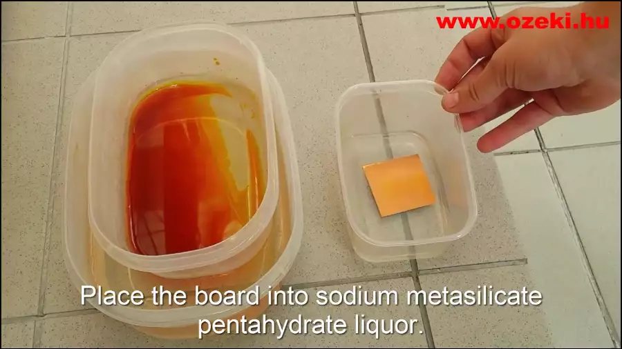
Step 1: Dip the board in sodium metasilicate pentahydrate
First you need to dip your copper board in sodium metasilicate pentahydrate to develop the surface which did not contacted with UV rays. Natrium hydroxide has the same effect if you cannot find sodium metasilicate pentahydrate. You should shake the liquid carefully from left to righ, straight and back and do this until you see your PCB design drawn out on the copper board.

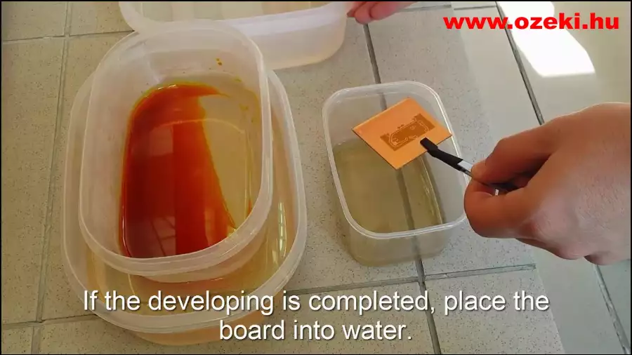
Step 2: Place the board in water
Do not touch the board with bear hands. Use a tweezer to dip it from one liquid to another. Now that the drawing of the circuit is developed, you will need to wash the sodium metasilicate pentahydrate from the surface. Dip it in water, shake it a bit and finally take it out from the water with the tweezer.

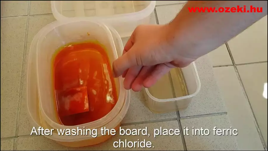
Step 3: Etch the board with ferric chloride
Place a bowl of hot water under a bowl of ferric chloride to keep it at 45 °C. Place your copper board in the bowl of ferric chloride. Do not forget to use a tweezer for this process. This liquid is a solvent which will eleminate the copper layer where there is no PCB circuit drawn. Please shake this liquid carefully until there is no copper surrounding the PCB circuit. You should see the plastic layer slowly visualizing under the copper. It is essential to watch the plastic layer because this step can take you from a few minutes to 2 hours.

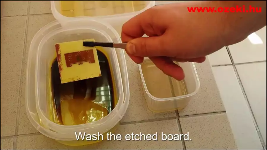
Step 4: Wash the etched board with water
When it is finished you should take it out with a tweezer and dip it in water. Shake the water and when you lift out the board you should see your copper PCB circuit just as you designed it.

More information
- Printing PCB front and back layer
- Making the packet
- UV exposure for PCB to prepare it for etching
- Developing and etching

 Sign in