How to design the schematics
If you ever dreamed of creating your own PCB boards then you can do it with this tutorial series. Before physically making the board you will need a plan. To draw the schematics of your plan you will need an electronics design software. This guide series is based on the open source KiCad.
Step 1: Start editing your PCB schematic
You shall start with downloading KiCad. After installation run KiCad from it's desktop icon. First create 'New Project' from the 'File' menu and determine the project location and name. Then click on the 'Electronic schematic editor' icon (Figure 1) to start creating your own design.

Step 2: Insert the required components and position them
Now start building your PCB schematic. KiCad has numerous components for example resistors, leds, transistors and microcontrollers. You can include these components in your designs. On figure 2 you can see which icon to click for choosing a component. When you have included all the available components move them to the right position. If you have every required component you can jump to step 4.

Step 3: Create your own component
In case you need a component that is not included in KiCad, you will need to create it by clicking on the icon shown in figure 3. When creating a component you just need to determine the size and configure the pins of the component. For the created pin you can choose from multiple electrical types starting with inputs and outputs. Finally insert the created component as shown in the video.

Step 4: Set names, wires and power flags
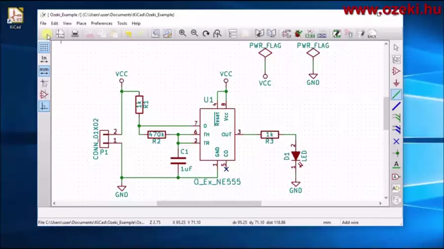
Now you shall see every component you will need, so please give them different names and values, for example a capacity of a condensator in farad. The names must be different so the program could distinguish them. A few important thing is still missing, one is wiring, so please connect the right pins. If you have a stand alone pin you need to indicate that you do not intend to use it. The other important thing missing are the power flags. You should connect every positive voltage and GND to a power flag, this way the program will know that these components have power flowing through them.

Step 5: Run the electrical rules checker (ERC)
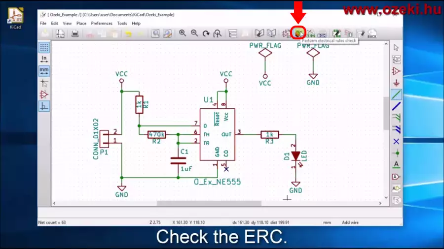
The schematic design looks ready (Figure 4) but we need to check if it is really ready for the next tutorial. Just click on the ladybird with the green tick on it to run the electrical rules checker (Figure 5). A window will pop up. Here you need to press 'Run'. If the message box stays empty and no error messages pop up then you have perfectly done your job. Although you can set the page settings like in the end of the video you can find on the top of the page.

More information
- How to design the schematics
- How to associate footprints to the components
- Designing your PCB

 Sign in