How to associate footprints to the components
Associating footprints to your components is the easiest part of this guide series. The footprint is essential for fitting and soldering a part onto the PCB. The tutorial video shows how to make a footprint for your new compontent if you have created one and how to pair the components already included in KiCad to the footprints. We are still in the electronic schema editor window.

Step 1: Create footprint for your new component (if any)
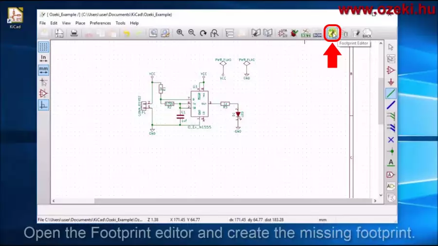
If you have not created a custom component in the last tutorial then you can jump to step 2. If you have created one then you need to design a footprint for it. To start designing please open the footprint editor (Figure 1). In the editor you should name the footprint, ad the pads to it and draw the frame of the component. Finally you should draw the marker of orientation by drawing a circle in one of the inner corner of the frame. If you are finished save your footprint in a footprint library.
Step 2: Open CvPCB to associate footprints to the components
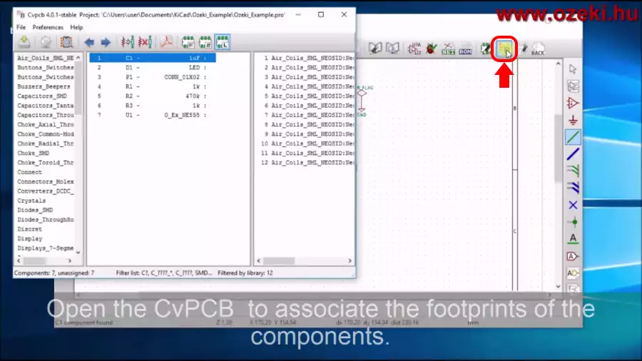
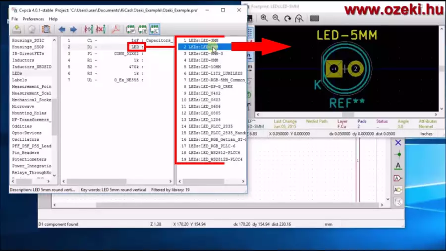
Here comes the main part where you associate the footprints to the components. To start association please open CvPCB (Figure 2). In the opened window you will see 3 columns from left to right: footprint libraries, the components you used in your schematic and the footprints pairable with the selected component (Figure 3).
Now you should start pairing the components in the middle column to the footprints in the right column. To see how your choosen footprint looks like (Figure 3) you should open the footprint viewer. In the middle column you should see the component-footprint pairs.
Reminder: If you have done step 1 then you should include your own footprint library into the library list. The footprint library list can be found in the left column.
Step 3: Run ERC just in case and Save netlist
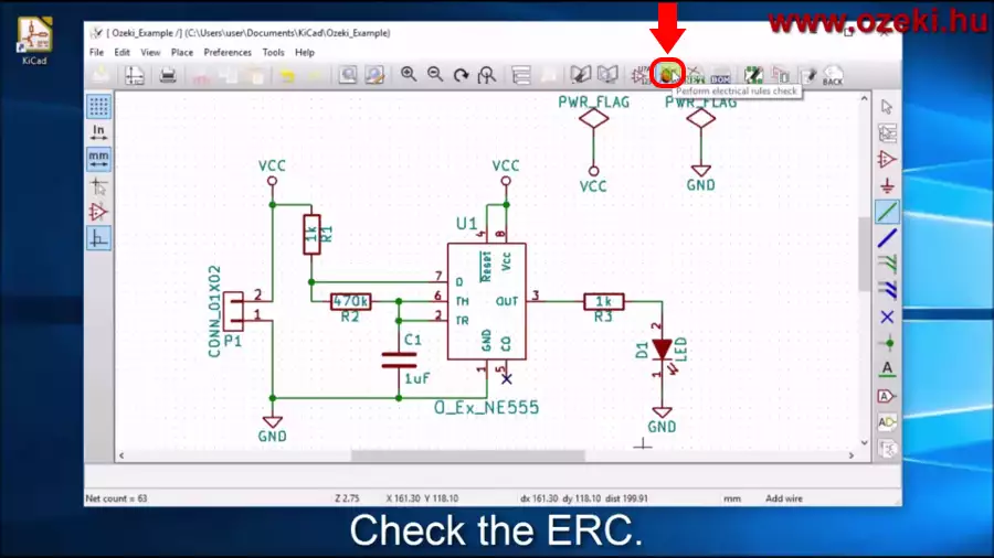
The schematic of the circuit should not normally change during this tutorial but you should run an ERC (electronic rules check) just in case something have changed (Figure 4).
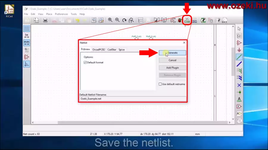
Now it is time to save your components, footprints and the component-footprint pairs you have previously associated. The netlist contains all, so you should generate a netlist (Figure 5). In the opened window click on 'Generate' and save the '.net' file.
You will see how to connect the footprint pads in the next tutorial
More information
- How to design the schematics
- How to associate footprints to the components
- Designing your PCB

 Sign in