Printing PCB front and back layer
If you finished designing your own PCB board the time has come to bring it to reality. In this tutorial you will see how to use KiCad to print the PCB layout to XPS files and how to send the XPS files to printer for printing on plastic foil. You will later need the foil for UV exposure.
Step 1: Print to XPS file
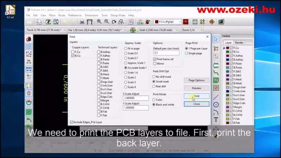
After opening your design in KiCad you should print the back and front layer of your PCB design to XPS files. When printing the back select 'B.Cu' and click 'Print' (Figure 1). Choose the folder and filename to print the file to. When printing the front layer make sure that you mirror it. Select 'F.Cu' and 'Mirror' before clicking 'Print'.

Step 2: Put foil in printer
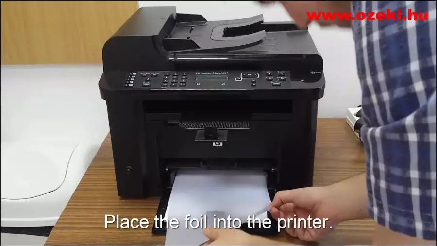
Choose a plastic foil as thick as a paper plane and lay it on your printer tray. The plastic foil must be transparent so later on you can do the UV exposure. It should smoothly lay on the white papers in your printer tray (Figure 2).

Step 3: Print to foil
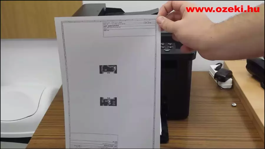
Print the front and back XPS files to the plastic foil you have previously inserted into your printer in step 2. First print the front then mirror the foil vertically and print the back. On figure 3 you can see a ready printing. In our next tutorial you will see how to make a packet from your freshly printed foil.

More information
- Printing PCB front and back layer
- Making the packet
- UV exposure for PCB to prepare it for etching
- Developing and etching

 Sign in